Continuing with the
investigation into the embodied energy that it takes to make an energy monitor, I thought I would explore in a little more detail the embodied energy of the microcontroller which is often associated with the most energy intensive aspect of electronics manufacture.
As I mentioned before I wouldn’t put a large amount of confidence in the accuracy of the figures below, computer chips are incredibly complex things that take a large number of manufacturing processes to make and I have found it hard to find open detailed information on energy requirements of these. The calculations below are based on the datasets that I could find including the EU
ecodesign dataset which I'm told is one of the higher quality freely available sources. But I could not find much detail on how the figures where derived to know what it does and does not include and the breakdown of energy use in its manufacture.
The idea here is more to get an initial set of numbers that could be improved upon in the future. My motivation for looking into this started by being inspired by
howies and
patagonia's efforts on footprint and supply chain analysis, partly by reading
sustainable energy without the hot air that identifies industry as being a significant part of overall energy use and also after reading the article here about
'the monster footprint of digital technology'.The following starts by looking at the available datasets and then investigates deriving figures for the embodied energy of a chip by calculation of the actual semiconductor volume contained which compares well for the small IC embodied energy value.
1) DatasetsEU Ecodesign methodologyThe EU ecodesign methodology downloadable here
http://ec.europa.eu/DocsRoom/documents/5308/attachments/1/translations/en/renditions/native provides embodied energy values for a variety of electronic component categories, it provides two embodied energy values for IC's (integrated circuits) these are:
Large IC 8021.88 MJ/kgSmall IC 1786.73 MJ/kgMJ/kg: 1,000,000 Joules per kg The question is what constitutes a small or large IC? Dimensions? processing power? and there is a large difference between both of these values!
Another paper that lists sources for embodied energy values including the EU ecodesign dataset is this paper on the embodied energy of an offgrid light
: http://users.humboldt.edu/arne/Alstone_etal_Lumina-TR9-Embodied-Energy_Jan11.pdf. It lists two other useful values:
Semiconductor Grade Si 35000 MJ/kg, Taiariol et al. 2001EPROM Chip (M27C1001, 0.36 W IC) 12.5 MJ/chip, Taiariol et al. 2001Jean Claude Wippler of JeeLabs did an interesting post a couple of years ago on what is inside an ATmega8 chip. The Silicon part was extracted by dissolving the outer casing with sulphuric and nitric acid.
http://jeelabs.org/2013/06/09/whats-inside-that-chipThe size of the semiconductor part inside the ATmega8 is 2855 x 2795 um, less than 3x3mm:
Is it possible to estimate the embodied energy of a microcontroller by working out the embodied energy of the silicon part and the casing part separately? and how would the figure compare with the embodied energy values given for a small and large IC in the EU ecodesign dataset?
ThicknessTo find the embodied energy of the silicon part we need to first work out the weight of that part. To do this we will need the density and thickness of the silicon wafer. The thickness of a silicon wafer can be anywhere between 275um and 926um.
Density of silicon: 2.3290 g.cm3 https://en.wikipedia.org/?title=Silicon
Weight2855 x 2795 um x 275 um = 0.00219 cm3 x 2.329 g.m3 = 0.0051 g2855 x 2795 um x 625 um = 0.00499 cm3 x 2.329 g.m3 = 0.0116 g2855 x 2795 um x 926 um = 0.00739 cm3 x 2.329 g.m3 = 0.0172 gThe embodied energy of silicon grade Si is around 35000 MJ/kg, 35 MJ/g
0.0051 g x 35MJ/g = 0.178 MJ = 0.049 kWh0.0116 g x 35 MJ/g = 0.406 MJ = 0.113 kWh0.0172 g x 35 MJ/g = 0.602 MJ = 0.167 kWhThe weight of a SMT Atmega 328 is 0.14375g:
Large IC: 8021.88 MJ/kg = 1.153 MJ = 0.320 kWhSmall IC: 1786.73 MJ/kg = 0.257 MJ = 0.071 kWhThe EPROM Chip (M27C1001, 0.36 W IC) example is 12.5 MJ/chip = 3.47 kWh
Which is between 10 and 50x the large/small IC estimates and 20 to 70x the wafer only estimates.
The large IC is between 2x and 6x the wafer only and small IC is between 0.5x to 1.5x the wafer only estimate.
The weight of the silicon part of the chip for the ATmega8 should be between 3.5% to 12% of the total chip weight.
The rest of the weight is metal and plastic. Copper has an embodied energy of between 38MJ/kg and 142MJ/kg depending on manufacturing process and plastic is anywhere between 80-120MJ/kg. If we assume a copper/plastic mix of around 100MJ/kg as a rough estimate.
This would then contribute an additional 0.0132 MJ = 0.0037 kWh which would only increase the embodied energy of the chip by around 2-7%.
Our estimate therefore for the embodied energy of the small microcontroller is between 0.053 kWh and 0.171 kWh, mid range of 0.117 kWh for 625um wafer which compares well with the small IC estimate of 0.071 kWh (it is of the right magnitude). We would expect a certain amount of assembly energy for combining the plastic, copper and semiconductor parts which is not included when taking a constituent parts approach which will likely add a little more to the total.
Package type?Calculating the embodied energy this way brings up an important question about the package type of the IC, I.e how much plastic and connector metal surrounds the semiconductor core. If the size of the semiconductor inside a through-hole and SMT version of a ATmega328 is the same then surely a total weight based measure is not a good guide for the embodied energy. Given that over 90% the embodied energy is associated with 3.5 - 12% of the weight.
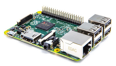
RaspberryPi chipsThe ATmega8 or ATmega328 is not a particularly powerful chip, the emonpi also uses a RaspberryPi which has three chips on board.
Its not clear what the volumes of the semiconductors inside these chips are. But given their small size and relatively large processing power lets assume for an initial calculation that the size of the package is very close to the size of the semiconductor. If the wafer thickness is 625um then the embodied energy of the chips can be estimated as:
Broadcom 14 x 14 mm x 625um = ~2.8 kWhElpida 12 x 12 mm x 625um = ~2.0 kWhSmst 8.7 x 8.7 mm x 625um = ~1.1 kWhThese estimates which cover a quad core 900Mhz + 1GB ram computer are much larger than the ATmega8 estimate as we would expect but are still significantly lower than the embodied energy figure given for the 32MB 2g memory chip referenced in the article on the
the monster footprint of digital technology of 20 kWh - while delivering much more functionality, almost a full computer!
Are these figures accurate? are the underlying datasets accurate for modern processors? Does it mean that newer miniaturised technology with the ability to pack much more computing power inside the same volume of semiconductor has resulted in a significant reduction in the embodied energy for equivalent amounts of computing digital technology functionality? These are all significant guesses at the moment and it would be really interesting and useful to see more open data available on the embodied energy of newer technology. It would be good to see greater interest from the manufacturers of these chips in calculating and giving information on the embodied energy of their products, making data available on this would really help with understanding this question about the impact of technology.


